Silicon can Match WBG Efficiency in Totem-pole PFC Circuits
Pressure is on engineers to design AC-DC power supplies with improved efficiency and power density, while meeting standards for mains harmonic emissions. The ‘totem-pole’ power factor correction stage is a key tool in achieving this goal, but a design using wide band-gap semiconductor switches is complex, with challenges to optimize control, gate drive, EMC, thermal management, and more. As a result, much time and effort can be expended to achieve often disappointing results using SiC or GaN.
This article describes a multi-level totem-pole PFC topology that leverages the simplicity and maturity of silicon MOSFETs along with a novel, modular approach to gate drives, achieving typically comparable efficiency and lower cost than traditional circuits using wide band-gap semiconductors.
Evolution of PFC Topologies
From 2001, power supply manufacturers in Europe saw a sea change in their industry, with the mandatory requirement to meet standard EN 61000-3-2, part of the European ‘EMC directive’. The standard limits the harmonic currents injected back into the AC line for equipment rated at 16A maximum, mandating power factor correction. The requirement is now global, with the US ‘Energy Star’ guidelines for example, setting similar standards.
The practical way to achieve compliance at higher power levels is with an active PWM circuit that forces the line current drawn to be near-sinusoidal. Although the conversion stage can take different forms, a ‘boost’ converter is preferred as it can work down to low input AC voltages and generate a regulated high voltage rail, where ride-through energy can be stored efficiently. This ‘boost PFC’ stage initially took the form of a line bridge rectifier and boost topology, Figure 1 (left). With demands for better efficiency, such as in the Energy Star ‘80 plus’ scheme, the circuit becomes unviable, with losses in three rectifiers conducting at any one time in the power train being too high, especially at low line. A solution proposed was the ‘totem-pole bridgeless PFC’ (TPPFC) topology Figure 1 (middle), where the conversion is split into two half-wave rectification phases. The boost switch and a synchronous diode formed by Q1 and Q2 swap functions on alternate polarities of AC input. D1 and D2 conduct at line frequency, so dynamic losses are insignificant, but they can be replaced by synchronous rectifiers Q3 and Q4 as in Figure 1 (right) for an incremental improvement in conduction loss. Q3 and Q4 are called the ‘slow’ switching leg, and Q1, and Q2 the ‘fast’ leg, are switched at high frequency. Control is complex, and there is only a limited selection of dedicated controllers, either analog or digital, but with optimization of the inductor and appropriate thermal management, good results are promised.
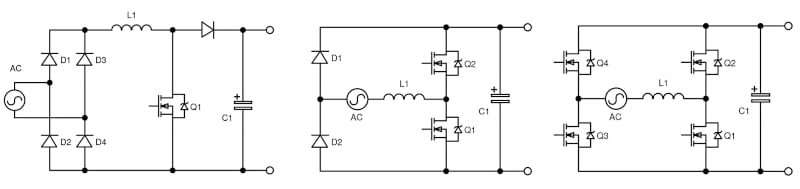
Depending on device selection, there are arbitrarily low voltage drops and conduction losses, but the TTPFC circuit proves unsuitable at high frequency and high power with silicon super-junction MOSFETs for the fast leg. This is because the topology normally operates in Continuous Conduction Mode (CCM) at high power levels for manageable peak currents. This, however, results in ‘hard’ switching, where the body diodes of Q1 and Q2 are forced to conduct. When they are subsequently forward biased, the high recovered energy of silicon SJ-MOSFETS causes excessive loss at high switching frequency and if the frequency is kept low to compensate, the inductor size and cost is unacceptable.
WBG Switches Promise a Solution, but…
Wide band-gap (WBG) semiconductors have been hailed as the answer to the issue, with SiC having low reverse recovery charge (Qrr) and GaN having effectively none. The devices do have downsides, though, particularly unit cost compared with Si-MOSFETs. The SiC body diode is fast, but still has a recovery charge and also a high forward voltage drop, around 3V. SiC MOSFETs still can have threshold instability issues that need to be screened out in manufacture at some cost and the gate drive needs to be around 18V for full enhancement, often close to the absolute maximum rating. GaN devices have a much lower gate threshold, making them susceptible to noise and have a low absolute maximum gate voltage of only around 7V. Gate drive is critical and with no gate oxide, as the threshold is exceeded, gate current flows and has to be controlled. GaN HEMT cells also have no avalanche characteristic, so over-voltages mean instant failure.
Both SiC and GaN have impressive switching speeds, but in practical circuits this makes PCB layout extremely critical and edge rates must be slowed to avoid unmanageable EMI and damaging voltage overshoots from parasitic inductance. Switching frequency in TPPFC applications with WBG devices is therefore often sub100kHz, not only for lower dynamic losses and better efficiency, but also to set the fundamental below the 150kHz lower limit of the CISPR22/32 conducted EMI emissions limit lines. With their listed downsides and without the benefit of small inductor size that goes with MHz switching of WBG devices, their attraction reduces somewhat, exacerbated by a lack of package standardization.
A Better, Multi-level Way
There is an alternative – as efficient as a WBG solution, but at lower cost and using standard silicon MOSFETs – the multi-level TTPFC (Figure 2).
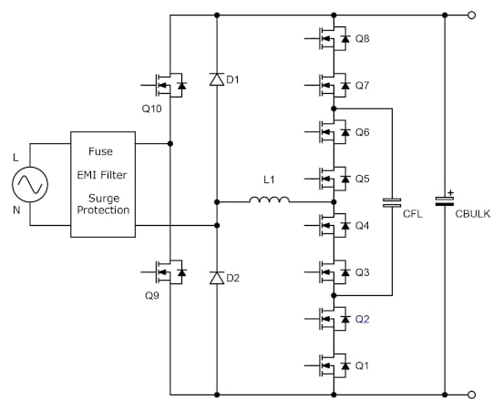
In this topology, the two fast FETs are replaced with two sets of four series silicon MOSFETs, which need only be rated at 150 V each for a 400 V DC output bus, allowing the use of multi-source parts with very low on-resistance and diode reverse recovery charge, yielding an overall loss comparable with a WBG solution. Two sets of two MOSFETs could be used but these would each need to be rated at 300 V which is uncommon, so two series-connected MOSFETs forming a composite device, e.g. Q1 and Q2 are driven on and off together. The switches in the leg are split into two groups: Q1, Q2, Q7, Q8 and Q3, Q4, Q5, Q6, and each group is driven in antiphase. When Q1 and Q2 are on, Q7 and Q8 are off and vice versa. Similarly, the drive signals for Q5 and Q6 are inverted versions of the drive signals for Q3 and Q4. The timing of the drive signals to the MOSFETs Q3 and Q4 (similarly Q5 and Q6) are a version of the drive signals to Q1 and Q2 (similarly Q7 and Q8) delayed by half a switching period. Regulation of input current and output bus voltage is achieved simultaneously by phase shift modulation of the drive to groups of MOSFETs at varying duty cycles, for example, between Q1/Q2 and Q3/Q4 (Figure 3).
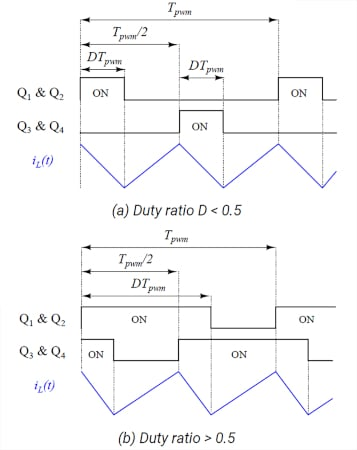
The inductor current plot illustrates a major advantage of the multilevel approach - compared with a conventional TPPFC, the inductor sees twice the frequency and half the voltage or, a quarter of the volt-seconds, which reduces inductor size to around a quarter, with a consequent cost and weight benefit. Typically, a low-cost ‘SendustTM’ core can be used. Differential EMI is also reduced by the lower volt-second product, leading to further savings in EMI filter size and cost.
The ‘flying’ capacitor CFL maintains half the bus voltage between Q2/3 and Q6/7 junctions, and balancing of the voltage across the series pairs can be ensured if necessary, by two further capacitors and clamp diodes, which dissipate no power in normal operation. Diodes D1 and D2 divert CBULK inrush current away from the inductor on start-up, to avoid magnetic saturation which would cause high initial switch currents.
Optimizing Power Semiconductors and Drives
Eight Silicon MOSFETs and isolated gate drives may seem daunting but the dissipated power is spread across the devices and they can therefore be small and surface-mount. For example, in a 3kW design, they might each dissipate just 2.5W, so can be typically in a small 5mm x 6mm ‘SuperSO-8’ package, and use PCB pads as heatsinks. In a two-level WBG implementation, heat is concentrated in hot spots in two devices that might need to be leaded, TO-247 for example, with extra assembly costs and reliability concerns.
Traditionally, options for gate drives have included bulky and expensive active circuits that need optocouplers for isolation and isolated power rails, often bipolar. In some schemes, pulse transformers can replace optos, but again for optimum performance, these are usually followed by powered drive stages. A solution that dramatically reduces size, cost and complexity is the IC70001 device from ICERGi in a tiny 2mm x 2mm U-DFN2020-6 package. This driver generates optimum gate drive waveforms from internal monostables with precision propagation delays, triggered on and off and powered by short pulses from an external transformer. The pulses are typically only 100ns duration, so the transformers are small with few turns. They can conveniently be implemented as planar types in the converter PCB and ICERGi can supply layouts for suitable designs using an EE style 4 x 7mm ferrite core. Only four transformers are actually needed as the MOSFETs are driven in pairs. The drives to the gates of each pair must still be mutually isolated, but this is achieved on the single transformer with separate windings, which can be on each outer leg of the E-core, achieving required isolation creepage and clearance. The small size and construction of the transformers also gives low isolation capacitance, necessary for good DV/dt immunity.
Optimizing Control
Obtaining highest efficiency and reliability depends on how the multi-level TPPFC stage is controlled and in the absence of a dedicated IC, ICERGi have developed proprietary firmware to run on a standard ARM Cortex-M0 microcontroller with minimal computational loading which, along with some specified external logic, performs all the necessary functions: power factor correction, regulation of output bus voltage and all necessary parameter sensing and protection features. For example, along with ‘smart’ overload, over-voltage and over-temperature monitoring, the firmware controls the flying capacitor voltage directly on start-up and under transient conditions, so voltage balancing between the MOSFETs is assured and their ratings are not exceeded. Use of an off-the-shelf microcontroller gives security of supply and extra features can be included as required, such as the drive to the ‘slow’ leg synchronous MOSFET gates or control and monitoring via a communications interface.
Performance Benchmarking
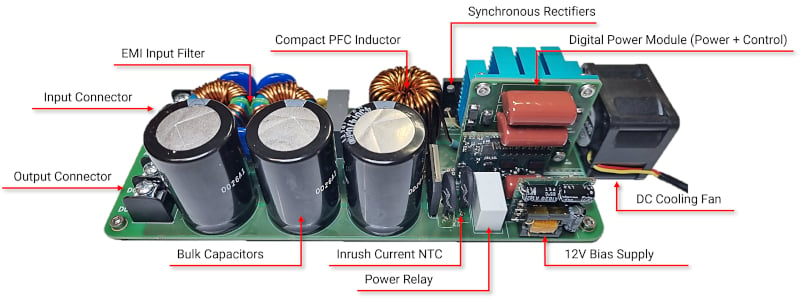
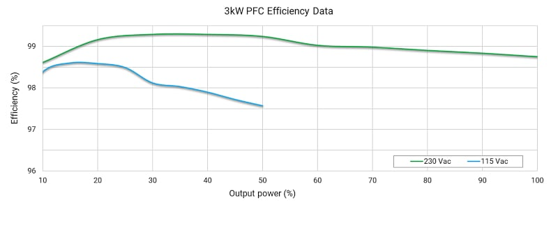
ICERGi has demonstrated the effectiveness of the multi-level TPPFC approach with its gate drivers and control firmware in reference designs and demonstrator boards. A version rated at 3kW with an input range of 85 VAC to 265 VAC, for example, achieves a power density of around 100/in3 for a complete functional unit with EMI filtering and auxiliary supply included (Figure 4). The unit shows an efficiency peaking at around 99.3% (Figure 5) while complying with IEC/EN 61000-3-2 for line current harmonics and EN 55022/32 conducted emissions limits, with 10dB margin.
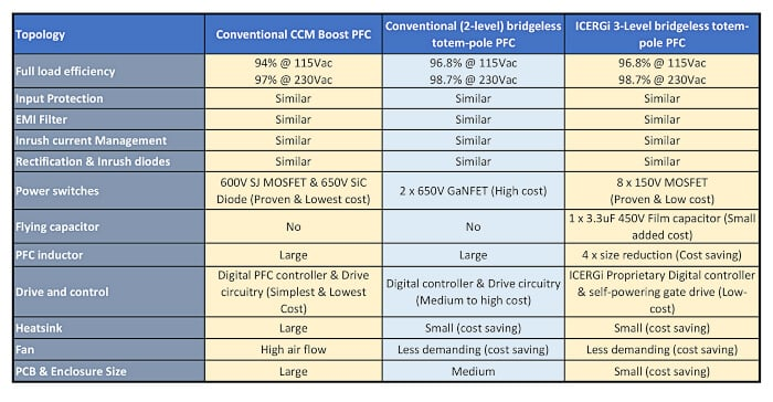
As a summary of the benefits of the design approach described, Table 1 compares the attributes of a conventional approach using a Si SJ-MOSFET plus SiC diode, a two-level GaN solution and the multi-level ICERGi solution. Perhaps the most telling comparison is between BOM costs - analysis by ICERGi shows a saving of 33% over GaN and 25% over SiC for comparable efficiency, including the license fee for the ICERGi firmware.
ICERGi have also packaged controllers, with their support components and gate drives, into various ‘pluggable’ modules which can be supplied for evaluation of the technology in customer designs.
Conclusion
The multi-level TPPFC approach with silicon MOSFETs can be as efficient as WBG solutions and lower cost, without resorting to interleaving to at least 3kW. Concerns about expensive, single source WBG devices are eliminated with the use of low-voltage off-the-shelf Si-MOSFETs and the self-powered drivers from ICERGi are an elegant, low-cost solution. Licensing ICERGi firmware allows designers to use commodity ARM processors as controllers, removing the reliance on single-source, dedicated ICs - an important factor in days of component allocation and supply disruption. In addition, reference designs make design-in easy, de-risking the R&D process and speeding end-product time to market.